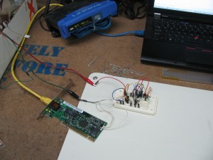
Reset-on-LAN: An ethernet-aware remote reboot device from junkbox parts.
What do you get when you mix an old 10/100 NIC, a handful of components, and a home server that goes off into the weeds once in a while? A network-connected reset button, and the ability to recover from the majority of mishaps! The concept is simple: Use a standalone NIC’s Wake-on-LAN capability to poke a different signal, specifically, the PC’s reset line. Best yet, the whole thing costs less than $3, and goes together in under an hour. Not too shabby, when you consider that comparable network-aware remote-reboot devices go for about $200!
The important realization behind the project is that a WoL-capable NIC can run standalone, given nothing but power. It seems so obvious in retrospect! This same concept could be easily used to drive an SSR for true cold-boot capability, interface with a UPS for output-disable, or other functions.
(UPDATE: There’s prior art! Their version is called “whack-on-lan” and uses a NIC without the retriggering problem, so their circuit is much simpler.)
Lots and lots of detail after the break…
Overview:
In this implementation, a scrap NIC is mounted in the PC’s case, not even plugged into the motherboard. It’s powered through its WoL header, but the wake output is routed through a simple edge-to-pulse converter circuit, to the motherboard’s Reset line. If I’m unable to VNC or RDP into the machine, I can SSH into my router and use command-line tools to send a magic wake-up packet to the RoL NIC’s MAC address, which resets the PC and, in the majority of scenarios, reboots it into a state where software-only remote-access tools work again. (If not, it’s likely that I’ll need to be on-site to effect repairs anyway, so an IP KVM or iLO/DRAC-style solution offers little additional functionality, and does not justify its cost.) Nota bene: This added NIC only accomplishes the reset-on-LAN task. The motherboard’s integrated GigE port is still used for network communication, and its own WoL capability can be used to wake the machine if it’s off for some reason.
This was one of those projects that kept me at the hackerspace well past go-home-and-sleep time, because I couldn’t stand to leave it unfinished. It sounds incredibly simple, and all the complexity stems from one simple awkward fact: When it receives a wakeup packet, the NIC asserts its wakeup signal, and keeps it asserted indefinitely. (Presumably until the OS loads a driver and initializes it?) But holding the motherboard reset line low indefinitely won’t reboot anything, it’ll hold the PC in reset forever — the reset signal needs to be driven with a pulse. Also, the NIC needs to be power-cycled somehow, so it’ll be ready to receive another wakeup packet in case another reset attempt is needed.
The circuit:
As a hobbyist who doesn’t spend much time actually building circuits, this involved a bunch of Googling and tinkering, so references are provided to most of the sources I used. It was incredibly fun, but I’ll be honest, the result is clumsy at best, and I fully expect someone to chime in with a more elegant, cheaper, simpler solution. Constructive criticism is always appreciated! I feel a bit embarassed to use an IC for this, but least there’s no Arduino wedged in here. 😉
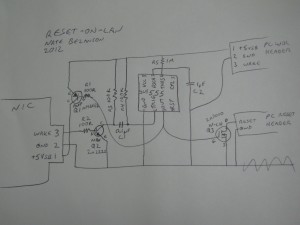
Power for the circuit comes from the PC’s PSU. This could be the +5VSB line coming off the motherboard’s WoL header, if it has one, or any other source of 5 volts — it shouldn’t much matter. The 555 timer starts up with its output driven low, so the gate of Q3 is held low, Q3 does not conduct, and the PC is not reset. The low output from the 555 also pulls current through the base (and base resistor R1) of Q1, turning it on and allowing power to flow to the NIC through pin 1 of its WOL header. The NIC wakes up, negotiates with the ethernet switch, and waits for a wake packet.
Also, R3 and R4 pull both sides of C1 high. The 555 is waiting for a low condition on its trigger pin 2, so it does not start a timing cycle. This is the idle state.
When the NIC receives a wake packet, it drives its output pin 3 high, which flows through R2 and the base-emitter junction of Q2, turning it on and pulling the left side of C1 to ground. (Actually, one diode-drop away from ground, so about 0.7v.) Capacitors oppose change in voltage across themselves, so the right side also goes low, pulling the 555’s trigger signal low, and starting a timing cycle. R4 now has a voltage difference across it, conducts, and charges C1. After a moment, C1 is charged enough that pin 3 is no longer triggered, meaning that the 555 will stop after it completes the current cycle. (This trigger circuit, and lots of background learning, from Dontronics.)
The 555 is connected as a monostable timer, and its output goes high as soon as the cycle begins. This enhances the gate of Q3 (driving it enough above the source potential that it begins to conduct), which pulls the PC’s reset signal low, and places the PC into reset.
Also when the 555’s output goes high, the voltage on Q1’s base approaches Vcc, emitter-base current goes to essentially zero, turning off the transistor and removing power from the NIC. As soon as the NIC’s internal power supply capacitance is depleted, the wake output signal falls and Q2 turns off, allowing R3 to bring the left side of C1 slowly back up to Vcc. Capacitors oppose change in voltage, so the right side of C1 is nudged slightly higher than Vcc, and drains back into Vcc through R4. In the Dontronics circuit, a diode is provided for this, which I have omitted. The momentary overvoltage is probably higher than the 555 wants to see on its trigger pin, but it doesn’t seem to hurt anything. Also, because this happens very quickly after the cycle starts, I don’t think C1 ever gets much charge anyway.
The 555’s period is set by R5 and C2, and is about 1 second. This is a fairly typical reset-button-press duration, and a sufficient power-down period to reliably reset the NIC. (An innocuous little sentence like that embodies unspeakable amounts of trial-and-error!) When the cycle completes, the output again goes low, which turns Q1 back on and depletes the gate of Q3, allowing the PC’s onboard pull-up to bring the reset signal high again. The NIC powers back up, and the PC comes out of reset. Hopefully, the PC boots into a state where it can be VNC’d into again!
No connections are made to the NIC’s PCI bus slot connector. Covering it with tape is recommended, to avoid inadvertent contact. (Presumably this would all work with a WOL-equipped ISA NIC too, but I didn’t have one handy to try.) If your PC case has more slot brackets than your motherboard has actual slots, mounting the NIC “past the edge” is straightforward.
Component choice:
To switch power to the NIC while keeping Ground connected, I needed a high-side switch, which in simple terms means a P-channel FET, or a PNP BJT, as Q1. The MPS6652 was handy, and boasts a continuous collector current rating of 1A, plenty of elbow room for the NIC’s needs. The 100-ohm base resistor should result in an emitter-base current of about 30mA, which when multiplied by the Hfe of 30-50, should allow 1A of emitter-collector current. (Update: BJTs inflict a diode worth of voltage-drop, but the NIC seems fine with this. Yours may not be. A P-FET would probably be better.)
Q2 could be any NPN BJT or N-channel FET, so I used the ubiquitous 2n2222. The choice of a 100-ohm base resistor was purely arbitrary and seems to work fine.
Values for R3 and R4 were chosen to be ten times higher, and C1 ten times smaller, than the Dontronics trigger example, to reduce current while keeping the relative values the same. Also, the smaller C1 hopefully reduces the potential for damage to the 555’s trigger pin, hopefully making the snubber diode unnecessary. I suspect that R3 could be made even larger, but have not tried it.
The 1-meg value for R5 was chosen to keep C2 small and cheap, while still allowing a sensible period for the timer. Shorter periods didn’t reliably reset the NIC, but one second seems adequate. Note that very-high resistances (beyond about 10 meg) can result in unreliable operation due to internal resistances within the 555 itself, so 1-meg is a good compromise and commonly available.
The use of a MOSFET for Q3 was mostly for fun; I don’t do enough with FETs and i3detroit’s electronics room had this drawer of 2n7000‘s just waiting for a use. The 2.1-volt gate threshhold is plenty of elbow room for a logic-level drive signal, and I love that the gate is capacitive and doesn’t need a base resistor. Every PC I tried seemed happy with the reset signal provided by the 2-ohm Rdson. Note that the FET can be connected in parallel with the existing mechanical reset button, and both should function normally.
A mating connector for the NIC’s WoL header was scavenged by cutting a WoL lead in half. The other half was used to get 5Vsb and Gnd from the PC’s motherboard. Connection to the motherboard’s Reset header reused standard 0.100″ pins, also scavenged.
Bill of Materials:
- LM555 in DIP-8: 87¢
- MPS6652: 16¢
- 2n2222: 20¢
- 2n7000: 25¢
- 5 resistors: 2¢ ea, 10¢ total
- 2 ceramic caps: 5¢ ea, 10¢ total
- electrolytic cap: 10¢
- Small perfboard: 80¢
- NIC: Scrap saved from the recycling bin, $FREE
- Total: $2.58.
(If implemented in surfacemount, the 555 drops to 20¢ and most of the transistors are around a nickel, so the whole BOM is under $1.)
Incremental costs of an additional network port and cabling would apply to a commercial network-reset device too, so these are not considered. Power consumption of the apparatus is presumed small and has not been analyzed, but is likely lower than a commercial standalone device, owing to the use of a separate PSU in such a setup.


Trackbacks & Pingbacks
[…] is a project that is a blatant rip-off… I mean derivative of a hack made by a friend of mine over at the i3Detroit hackerspace. His hack used the Wake On Lan feature […]
Leave a Reply
Want to join the discussion?Feel free to contribute!